K-1008 replica update
I’ve realised that I’ve completely messed up the schematic. The RAM chips are connected together in the most efficient way for the layout, not according to their intended pinout.
For example, A1 in the MM5280 is pin number 9, but the A1 line of the board is connected to pins 8, 10, 13 or 15 depending on the chip. It doesn’t really matter because you are getting an unique address on each chip and it makes the layout and routing much easier, but it is a nightmare when you try to follow the schematic.
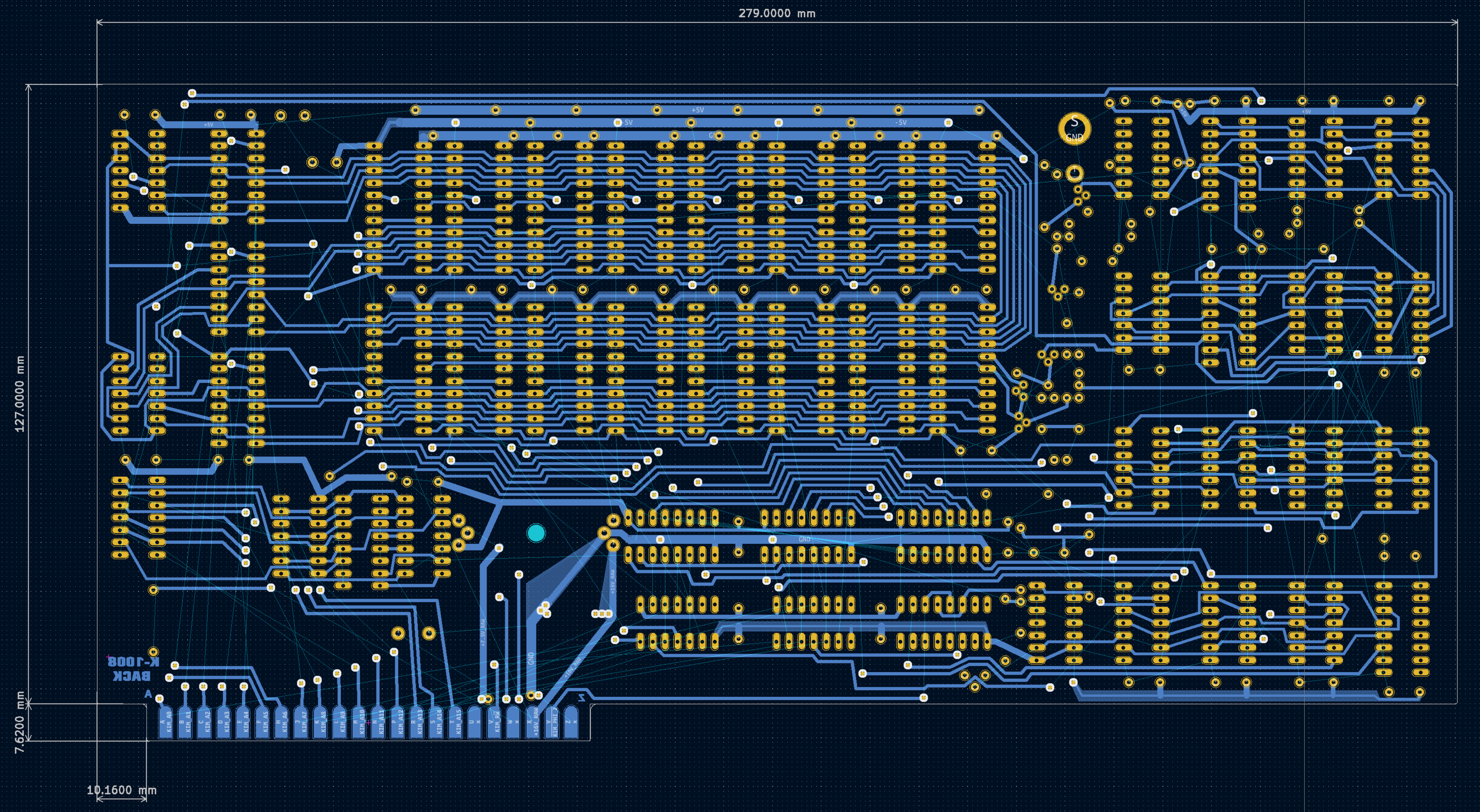
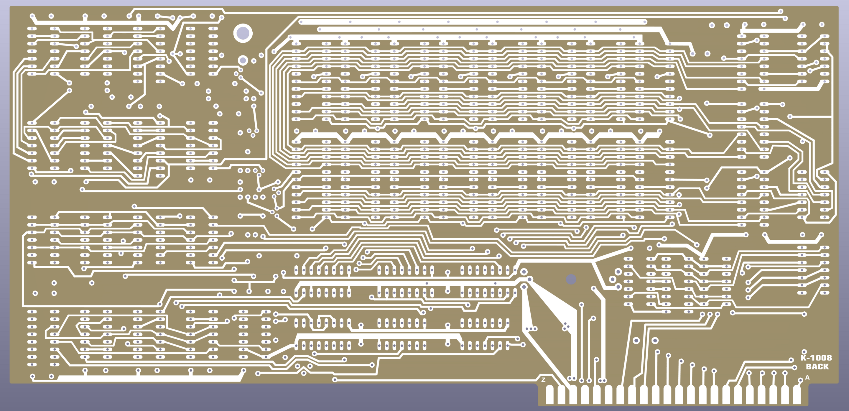
With that corrected, I’m halfway there and routing of the bottom layer is completed.
This post is licensed under CC BY 4.0 by the author.

